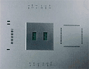
Used when printing the pattern with small and large apertures at one time
. (Large ones need enough amount of paste, but small ones need less for
avoiding the “bridge”, “solder ball spreading” problems.)
Or when PCB has some parts of 凸 , used as covering ( avoiding contact) so that
flat contact with stencil and PCB can be obtained.
Features
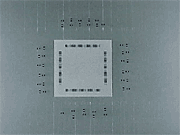
Overall-step down
(remaining small area 凸)
Adequate amount of paste for both large devices and small devices.
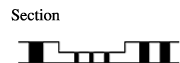
section
Ex)thickness=combination of 0.25/0.15mm
Small area step down
By making specified thickness in fine pitch pattern area, proper amount of paste
can be supplied to the area.
Features of step down stencil
application
Electro-forming, laser-cutting, chemical etching stencil
Lead time
1day extra adding to normal schedule for each stencil