Electro-forming stencil
Cavity stencil
Features
It enables to finish both solder applications in one printing process and shorten the tact time.
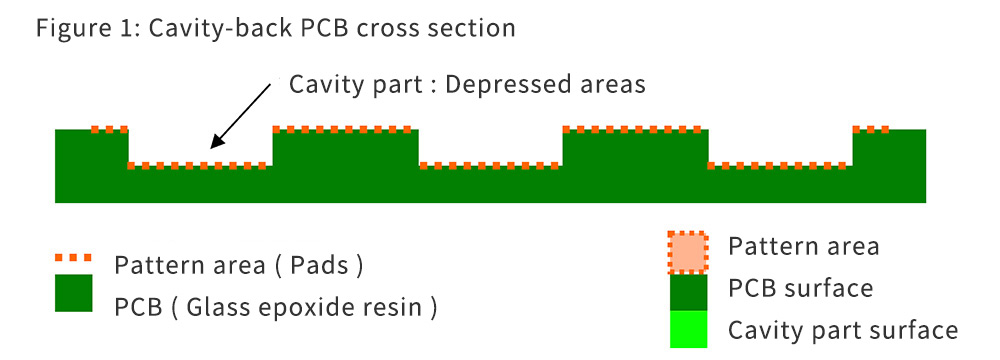
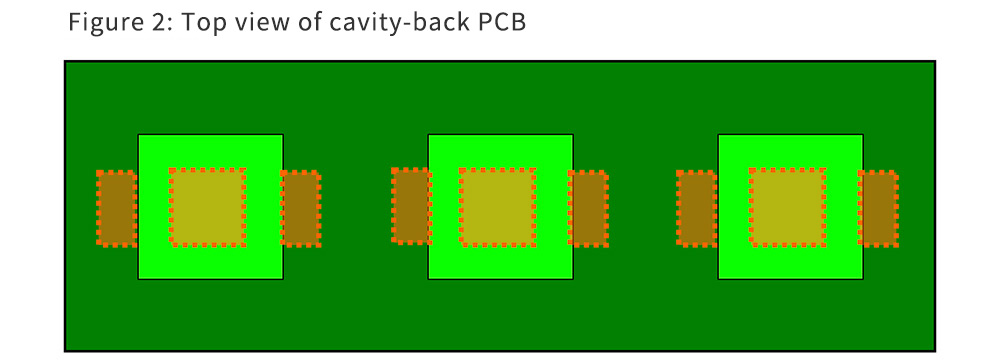
Cavity-back PCB illustration
The cavity-back PCB is characterized by its uneven surface
Conventional printing method of cavity-back PCB by the standard stencil
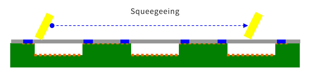
The standard stencil is flat; hence, we need to divide solder paste transcription into two processes
1.First process: Stencil printing on the PCB surface
Stencil printing by the printing machine
2.Second Process: Apply solder paste on cavity surface by the dispenser machine
Use of dispenser machine, manual printing etc.
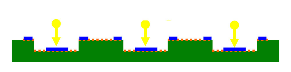
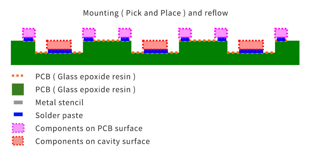
3.Mounting ( Pick and Place ) and reflow
4.Demerits of conventional printing method by the standard stencil
- It requires two processes
- It also requires two machines and burdens big machine spaces
- The limitation of precise solder application by the dispenser process
- longer tact time for manufacture
New method by Bon Mark Cavity stencil
Our cavity stencil enables you to print both PCB surface and cavity part at once by the printing machine
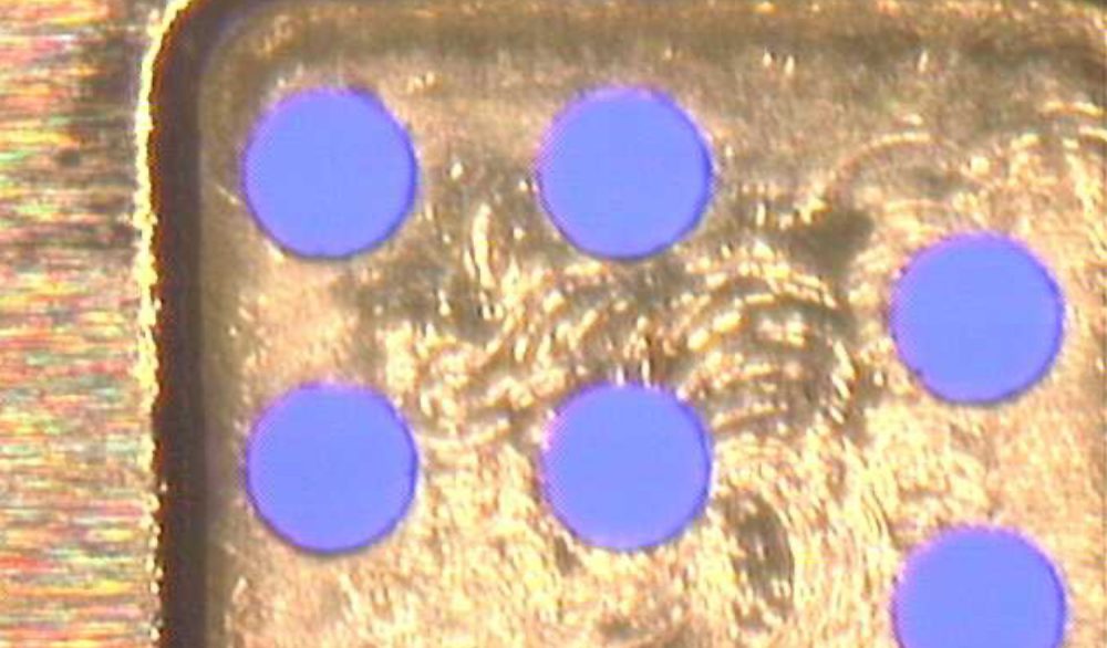
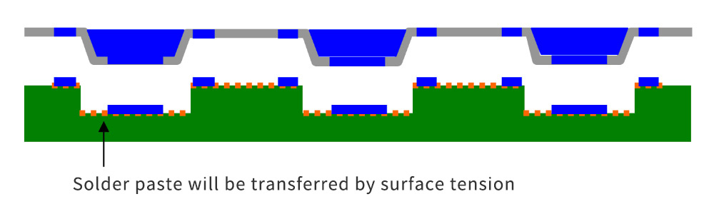
Cavity stencil printing by the printing machine
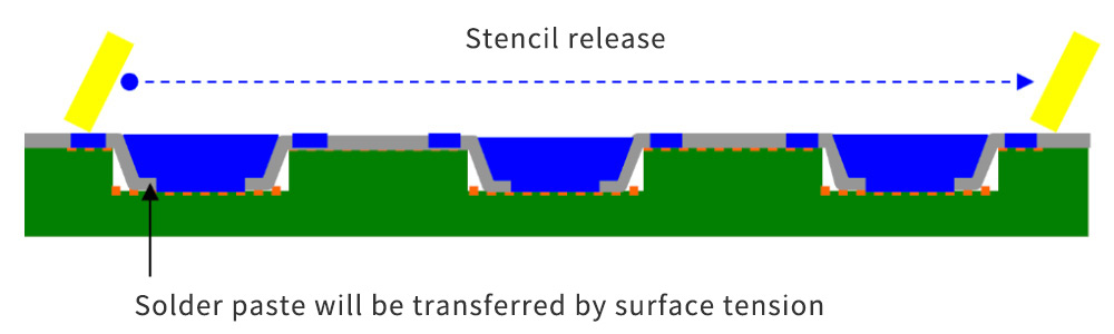
Stencil release
Mounting ( Pick and Place ) and reflow
Merits of Bon Mark cavity stencil application
- It enables to finish both solder applications during one printing process
- It requires only printing machines and saves the factory space
- It may achieve very precise pattern printing on the cavity surface rather than dispensing
- It enables to shorten tact time