Electro-forming stencil
Fine-pitch stencils for semiconductors and electronic components
Features
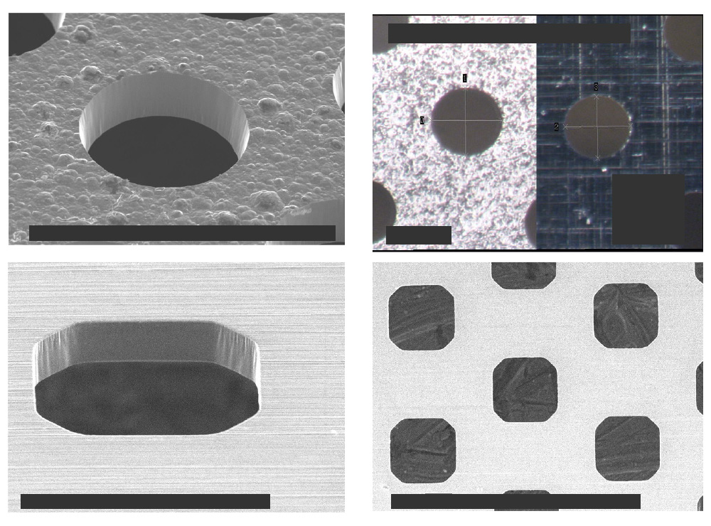
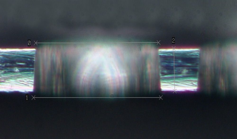
- Our photolithographic technologies, such as exposure, development and stripping achieve high-quality and precise stencil apertures.
- Precise and acurate aperture shape
- Smooth opening wall surface
- intentional rough surface finish on stencil backside for excellent stencil release
- High cost performance can be achieved for high density patterns with a huge number of opening apertures.
Applications
- C4 pre-solder bump printing for IC substrate and wafer
- Flux printing for IC substrate ( IC package ) and wafer
- VIA hole filling for ceramic capaciters
- Printing for ultra-small component modules
- Sieving Stencils for solder ball inspection and sorting
- Vapor deposition and vacuum evaporation stencils for OLED
- Widely used in various applications.