〜optimum for high dense & fine pattern〜
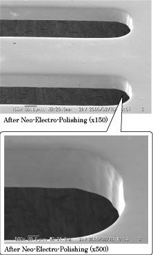
Realization of ideal laser-cut stencil . Aperture s’ inside wall roughness
,which may hinder paste performance, has become smoother and flat as possible
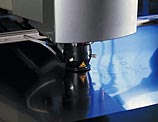
by special process being done after cutting
Inside wall surface of Neo
In
normal stencil, there can be seen many dross on the surface of inside wall after
laser-cutting. And usually they will be removed for the better printing.
We’ve taken further step for this, not only removing dross or burr, but also
improving its flatness & smoothness for the smaller device printing coming ahead
near future.
 In
normal stencil, there can be seen many dross on the surface of inside wall after
laser-cutting. And usually they will be removed for the better printing.
In
normal stencil, there can be seen many dross on the surface of inside wall after
laser-cutting. And usually they will be removed for the better printing.