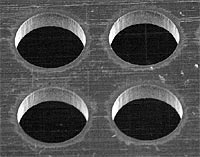
At the beginning, started by producing Etching Stencils, now our stencil
technology has so upgraded that we can supply the stencil for forming bumps
on wafer(wafer-level CSP). This requires our factory with more strict quality
controls and made it possible for us to produce the stencil accurately
[stencil with smaller aperture(such as Ф30um) and with thickness (15um
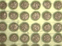
) ] Considering the technology trends of packaging, the terminals
will become
finer in their pitch and increase their numbers in the limited area, resulted
from which LSI will be smaller and smaller with terminal pins increased.
BON MARK are pleased to propose to the customers, stencil available for
0402 [mm] chip ( by inch: 01005), 0.15mm, 0.10mm pitch pad in wafer-level
CSP.
Ultra Thin Stencil
For the better paste’s release performance, inside-aperture wall’s
surface form has been improved.
Capable for ultra thin foil thickness, and even for ultra fine aperture
diameter.
And we can also offer special type stencil by combination with other
technology.
For the details,
Please inquiry to our sales staff first.
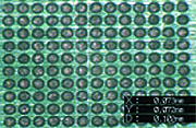
 Considering the technology trends of packaging, the terminals
will become
finer in their pitch and increase their numbers in the limited area, resulted
from which LSI will be smaller and smaller with terminal pins increased.
BON MARK are pleased to propose to the customers, stencil available for
0402 [mm] chip ( by inch: 01005), 0.15mm, 0.10mm pitch pad in wafer-level
CSP.
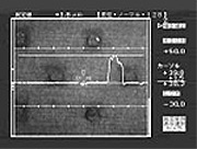
Considering the technology trends of packaging, the terminals
will become
finer in their pitch and increase their numbers in the limited area, resulted
from which LSI will be smaller and smaller with terminal pins increased.
BON MARK are pleased to propose to the customers, stencil available for
0402 [mm] chip ( by inch: 01005), 0.15mm, 0.10mm pitch pad in wafer-level
CSP.